
Breakthrough in black phosphorus research paves the way for next generation electronic and optoelectronic devices
Other Articles
Black phosphorus (BP), a rising star in the family of two-dimensional materials, plays an important role in improving the performance of information devices. BP is a layered semiconductor with controllable bandgap and high carrier mobility. It is an ideal candidate for applications ranging from nanoelectronics and nanophotonics to quantum devices and superconductors. However, the inability to produce ultra-thin BP films on a large-scale has previously hindered its development and application prospects.

Professor Hao Jianhua
To overcome this long-standing obstacle, Professor Hao Jianhua, Chair Professor of Materials Physics and Devices and Associate Head of PolyU’s Department of Applied Physics, and his research team have developed a technique to synthesise ultra-thin BP on the centimetre scale through pulsed laser deposition (PLD). PLD is a method used to fabricate thin films through evaporating materials using laser pulses. The team experimented with the method for five years and succeeded in making highly uniform BP films with an area large enough to be compatible with commercial fabrication methods. The research findings were detailed in the paper “Large-scale growth of few-layer two-dimensional black phosphorus”, which was recently published in the world-renowned science journal Nature Materials.
The breakthrough paves the way for further developing BP-based centimetre-scale devices with potential applications in the information industry.
“By using the PLD, we increased the size of the few-layer BP from dozens of micrometres to the centimetre scale,” Professor Hao explained. This opens up enormous application prospects for the material. For example, BP has the potential to replace silicon to make transistors of a much smaller size — with the thickness of just a few atoms. “That means we can fit a much larger number of transistors, probably a thousand times of what existing technology allows, into intelligent electronic devices, like mobile phones and computers, to enable faster and more powerful functions.”
Using the pulsed laser deposition (PLD) process to produce large-scale ultra-thin black phosphorus (BP) films compatible with commercial fabrication methods
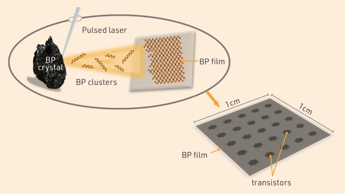
(Top) The research team strikes a piece of BP crystal with laser pulses inside a vacuum chamber to generate clusters that can settle on a surface to form ultra-thin BP film on the centimetre scale.
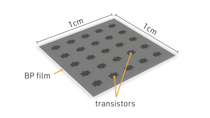
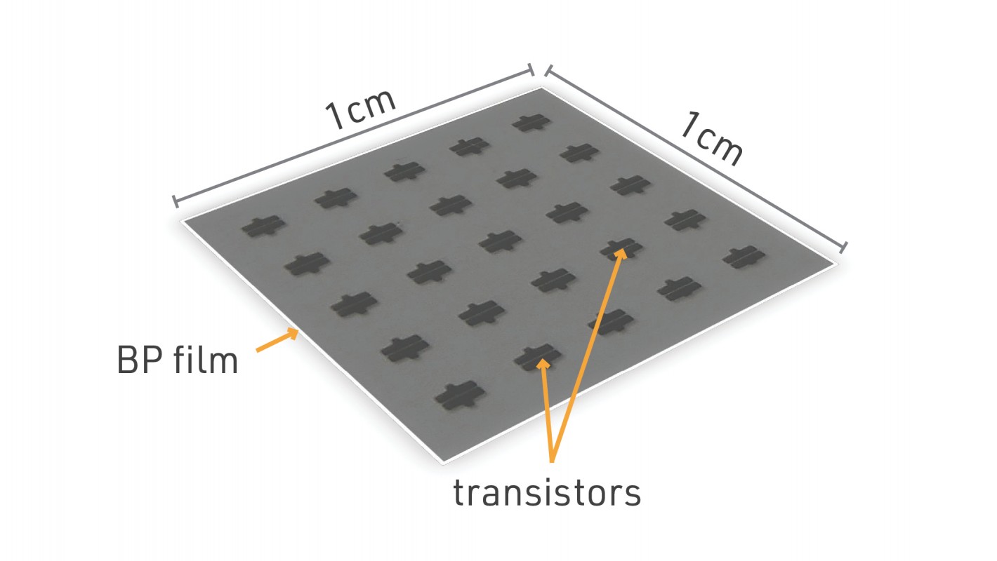
(Bottom) An example of the BP film produced through this technique – a sheet of 1 cm2 BP film that can accommodate 25 transistors with good electrical performance for use in electronic devices.


