Introduction:
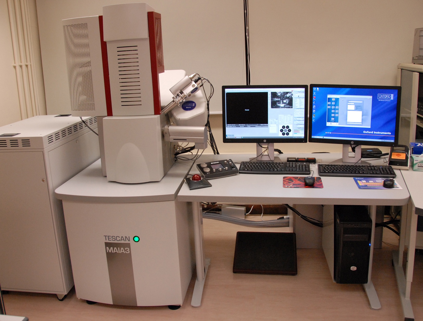
Field Emission Scanning Electron Microscope (FESEM), type of electron microscope in which electrons are drawn from the source by a high electrical field, focused to scan and study surfaces of solid objects. The TESCAN MAIA3 is a high-performance FESEM system that features a high-brightness Schottky emitter for high-resolution and low-noise imaging. The system has excellent imaging capabilities in the whole range of beam energies and is suitable for resolving nano-sized features in samples. It provides enhanced surface sensitivity and image contrast at low beam energies. MAIA3 also features Beam Deceleration Technology (BDT), which enhances the electron column performance by reducing optical aberrations, allowing small spot sizes and high-resolution imaging at low energies.
MAIA3’s versatile detection system and high spatial resolution allows the observation of even the finest surface details. This is an essential feature for comprehensive characterization of nanomaterials and observation of beam-sensitive samples with the best topographic contrast and detail.
Specifications / Applications:
- Unique column design, combination of three-lens objective and crossover-free beam path
- Imaging up to 500,000x with STEM option installed
- High brightness Schottky field emission source
- Large chamber size: 285 mm (W) x 340 mm (D)
- Compucentric 5-axis motorized specimen stage
- Fully integrated chamber and column active vibration isolation
- Chamber view camera
- Turbomolecular pump for fast pumping
- YAG crystal SE detector
- In-Beam SE detector, located inside the column to detect high angle signal, enables detection of electrons at very short working distances
- Retractable four quadrant YAG scintillator crystal BSE detector
- STEM detector module extends the imaging capabilities by simultaneous acquisition of multiple signals from transmitted and diffracted electrons, including bright field, dark field and high angle dark field
- Beam Deceleration Technology (BDT) allows imaging at low electron landing energies, down to 50 eV
- Oxford Energy-dispersive X-ray (EDX) and Wavelength-dispersive X-ray (WDX) spectroscopy system for elemental analysis
Notes to user:
Any vacuum compatible solids (thin films, powders, fibers, bulk materials) for SEM. For EDX sample, same requirements as SEM but highly polished surface is recommended.
Supplier information:
http://www.tescan.co.kr/product/em/em03
Please click here to download the equipment introduction poster.
Equipment location:
Room BC710