


Introduction:
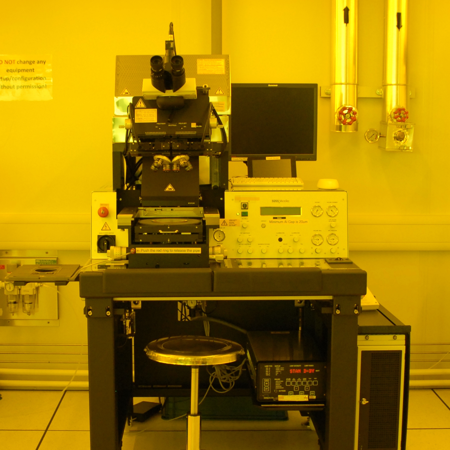
A UV mask aligner is a key photolithography tool used in semiconductor device fabrication and microfabrication to transfer microscale patterns onto a substrate. The system uses ultraviolet (UV) light to project a predefined geometric pattern from a photomask onto a substrate coated with a light-sensitive material known as photoresist. During exposure, the UV light induces chemical changes in selected regions of the photoresist according to the photomask pattern. After development, the patterned photoresist acts as a protective or sacrificial layer for subsequent fabrication processes. Depending on the process design, the transferred pattern can be used for wet or dry etching, thin-film deposition, lift-off, ion implantation, or other microfabrication steps. Precise alignment between the photomask and existing features on the substrate enables the fabrication of multilayer device structures. UV mask aligners are therefore widely used in the fabrication of semiconductor devices, microelectromechanical systems (MEMS), sensors, microfluidic devices, and other micro- and nanoscale structures.
Specifications:
- Light source: Hg 350W UV light
- Resolution: <0.8µm max.
- Exposure Modes: Soft / Hard / Vacuum contact
- Alignment: Top side alignment
- Substrate: Up to 4” round wafer
Notes to user:
Supplier information:
Please click here to download the equipment introduction poster.
Equipment location:
Room HJ705 (Class 100)
