Introduction:
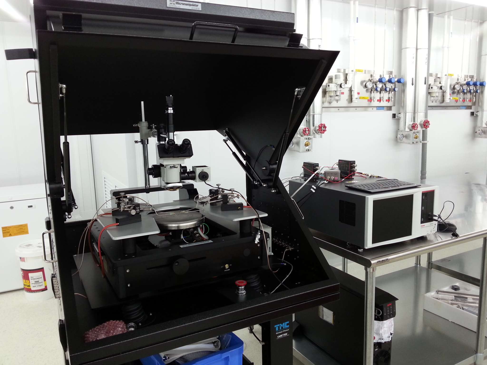
A probe station is used to physically acquire signals from the internal nodes of a semiconductor device. The probe station utilizes manipulators which allow the precise positioning of thin needles on the surface of a semiconductor device. If the device is being electrically stimulated, the signal is acquired by the probe and forwarded to analyzer. The probe station is often used in the semiconductor devices characterization on wafer level and before packaging.
Specifications:

- Substrate size: Up to 6” wafer
- Magnification Power: 0.7 → 4.5X, 10X eyepiece
- Aluminum platen: Fixed and stable
- Thermal chuck: max. 400°C
- Measurement: DC I-V, C-V, pulse and ultra-fast I-V testing
Notes to user:
Supplier information:
https://www.micromanipulator.com/
https://www.tek.com/keithley-4200a-scs-parameter-analyzer
Please click here to download the equipment introduction poster.
Equipment location:
Room HJ705 (Class 1,000)