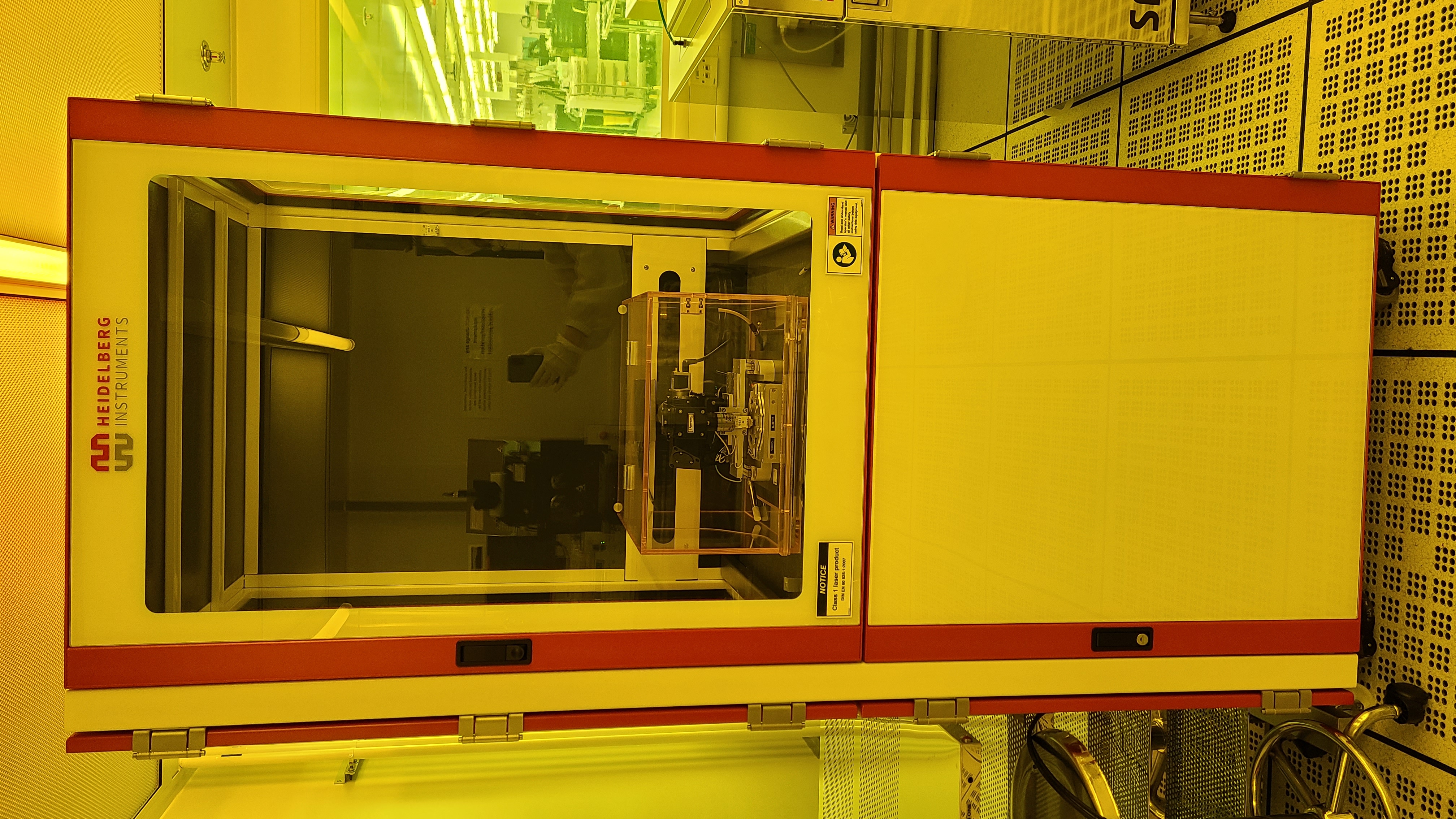
Introduction:
The Heidelberg Nanofrazor is an advanced nanofabrication tool designed for high-precision patterning at the nanoscale. The Nanofrazor utilizes thermal scanning probe lithography (t-SPL) technology to directly write intricate nanostructures onto a substrate with exceptional accuracy and resolution. This tool is particularly valued for its ability to create complex 3D nanostructures and its versatility in working with a variety of materials. The Nanofrazor is widely used in research and development across fields such as nanotechnology, materials science, and electronics, enabling innovations in areas like quantum computing, photonics, and biomedical devices. Its precision and flexibility make it a powerful instrument for pushing the boundaries of nanoscale engineering and fabrication.
Specifications:
- Substrate size: 1 x 1 mm2 to 100 x 100 mm2
- Substrate thickness: up to 10 mm
- Patterning size: minimum 15 nm
- Lines and spaces: minimum 25 nm
- Writing field size: maximum 60 x 60 µm
- Write speed (typical scan speed): max. 1 mm/s
- Write speed (50 nm pixel): max. 1000 μm2/min
Notes to user:
Supplier information:
https://nanofrazor.com/nanofrazor/
Equipment location:
Room HJ705 (Class 100)