Introduction:
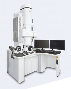
The JEM-F200 is a multi-purpose 80/200 KV field emission analytical electron microscope. The thermal electron field emission electron gun (TFEG) produces a highly stable and bright electron probe. This feature is essential for ultrahigh resolution in scanning transmission microscopy and in an analysis of a nano-scaled sample. Various analytical instruments such as dual EDS (Energy Dispersive X-ray Spectrometer), BEI (Backscattered Electron Image Device), and Clearview camera with in-situ capabilities are integrated.
Applications:
- Bright Field (BF) Imaging: Conventional TEM imaging mode for observing sample morphology, structure, and defects with high contrast.
- Dark Field (DF) Imaging: Enhances contrast for specific crystallographic orientations or defects by selecting scattered electrons.
- High-Resolution TEM (HRTEM): Atomic-scale imaging for lattice structure analysis and defect characterization.
- Scanning Transmission Electron Microscopy (STEM): High-resolution imaging and analytical mapping using focused electron probes.
- Selected Area Electron Diffraction (SAED): Crystallographic analysis of specific regions within the specimen.
- Convergent Beam Electron Diffraction (CBED): Precise determination of crystal symmetry, lattice parameters, and strain mapping.
- Nanobeam Electron Diffraction (NBED): Localized diffraction analysis for nano-sized regions, enabling phase identification and strain measurement.
- Energy Dispersive X-ray Spectroscopy (EDS): Elemental composition analysis with high spatial resolution.
- Backscattered Electron Imaging (BEI): Z-contrast imaging for compositional and topographical information.
- In-situ Experiments: Real-time observation of dynamic processes such as heating, mechanical deformation, or chemical reactions within the microscope.
Notes to users:
Inexperience users of the TEM are required to get training from the laboratory supervisor. Any first-time user of PolyU-CEM is required to be trained for microscopy skills.
Specimens should ideally be less than 100nm in thickness, prepared carefully to minimize specimen contamination.
Magnetic bulk samples containing iron, cobalt, nickel, or neodymium are fobbiden. If magnetic samples are concealed or tested without authorization, resulting in damage to the pole shoes, the user will be responsible for all repair costs. By making a reservation, you agree to the above terms.
Supplier information:
https://www.jeol.com/products/scientific/tem/JEM-F200.php
Equipment location:
Room CF002