
New transistor breaks a fundamental limit standing in the way of energy-efficient chips
The next generation of microelectronics relies on improvements in transistor switching performance to advance computing power. However, conventional semiconductor technology has hit the physical “Boltzmann limit”, which restricts the energy efficiency of traditional transistors. A research team at PolyU has engineered a novel tunnelling field-effect transistor (TFET) utilising 2D nanomaterials. The breakthrough can offer the fundamentals for energy-efficient computing and next-generation AI chips.
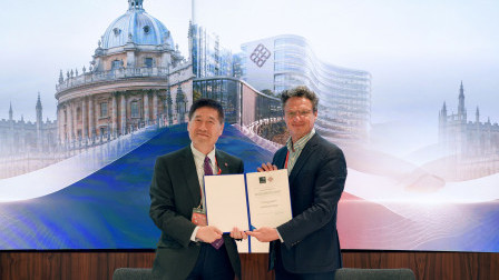
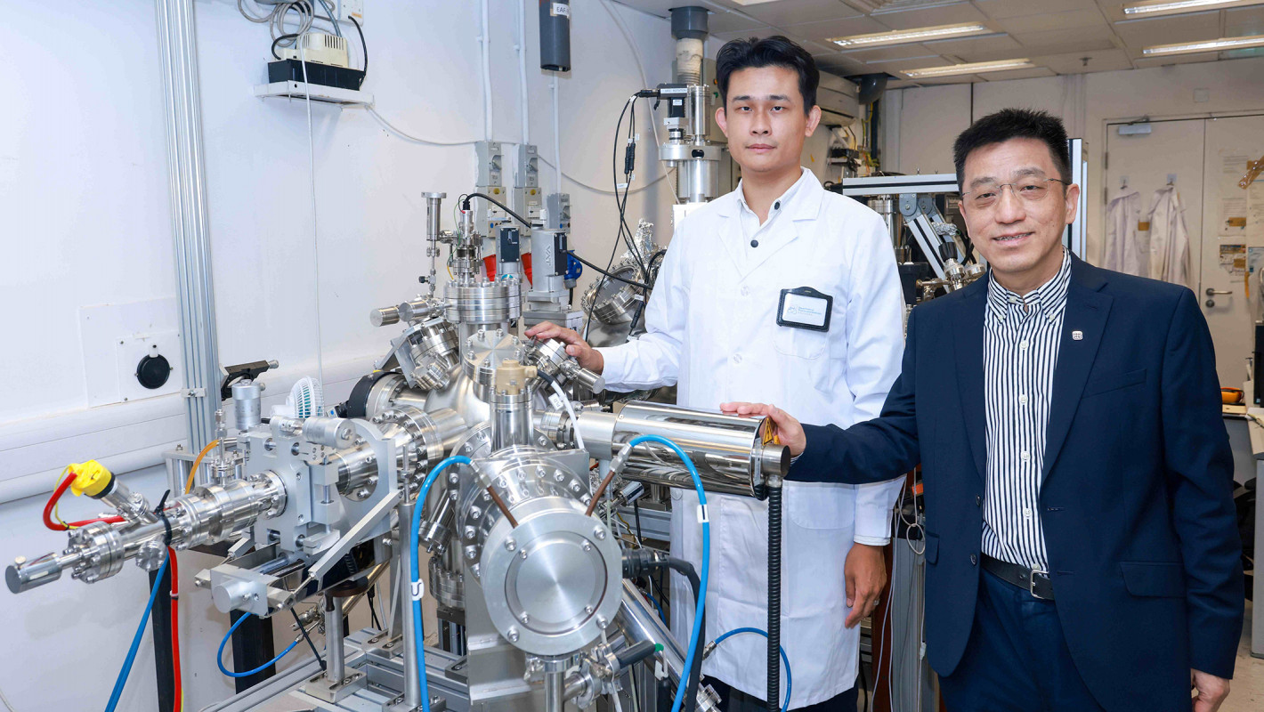
The research was led by Prof. Jianhua Hao, Head of the Department of Physics and Materials and Chair Professor of Materials Physics and Devices at PolyU, in collaboration with the National University of Singapore, The Hong Kong University of Science and Technology, Peking University, and the Singapore University of Technology and Design. The findings have been published in the prestigious scientific journal Science.
Conventional transistors rely on thermionic emission of electrical charges over a barrier. However, the “Boltzmann limit” makes it physically impossible for their subthreshold swing — a measure of switching efficiency — to fall below 60 mV per decade of current at room temperature, capping progress in high-performance electronics.
Prof. Hao explained that by adopting quantum tunnelling, the TFET breaks through this boundary, paving the way for ultra-low-power, high-performance integrated circuits essential for emerging AI chips and advanced semiconductor applications.
Turning a metal into a semiconductor
To overcome the limits that hampered earlier TFET designs, the team built an ultra-thin structure of alternating layers of 2D bismuth and indium selenide (InSe) using pulsed laser deposition (PLD). By controlling the layers with nanoscale precision, they coaxed bismuth — normally semi-metallic — to behave as a semiconductor in its 2D form, creating the ideal energy alignment for charge carriers to tunnel efficiently into the InSe.
The resulting Bi/InSe device achieved switching values well below the 60 mV decade⁻¹ limit across six orders of magnitude of current. Running at room temperature on standard centimetre-scale silicon, it needed a gate-voltage range of just 160 mV — a fraction of the 800 mV demanded by advanced MOSFETs.
Crucially, the device also solved a stubborn problem in experimental TFETs, delivering a high output current of several microamps per micrometre alongside an exceptionally high ON/OFF ratio. That combination is essential for driving multiple downstream logic gates, reducing circuit delay and ensuring compatibility with, and even upgrades to, existing chips.
A scalable path to greener AI hardware
The study further shows that PLD is viable for high-precision, wafer-scale production of the 2D materials prized for transistors with ultra-short channels. Because the process integrates seamlessly with traditional silicon manufacturing, the breakthrough offers an effective, scalable roadmap for the energy-efficient microchips set to power the AI era.