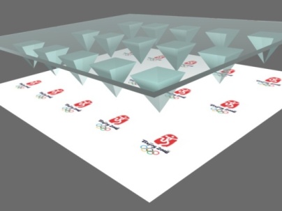
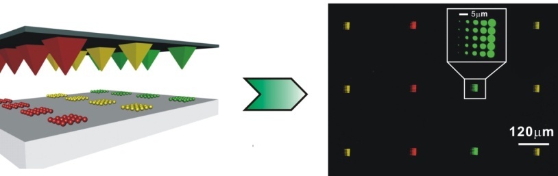
1. Surface patterning |
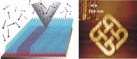
Patterning is of paramount importance in many areas of modern science and technology, ranging from the productions of semiconductor devices to biochips for medical diagnostics. We are interested in developing nanotechnologies and tools for surface patterning at the nanometer scale. Currently, we will focus on developing novel scanning-probe-based approaches, including dip-pen nanodisplacement lithography (DNL) and polymer pen lithography (PPL). DNL is a high resolution, high registration, program controllable, solution-free, and diffusion-limited lithography tool for simultaneously destruction and construction of molecules on a surface in air and ambient conditions at the nanometer scale.
|
| |
| Recent Publications |
|
Programming Nanostructures of Polymer Brushes by Dip-Pen Nanodisplacement Lithography (DNL)
X. Liu, Y. Li, Z. J. Zheng*, Nanoscale, 2010, 2, 2614. |
|
| |
|
Polymer Pen Lithography
F. Huo, Z. Zheng, G. Zheng, L. R. Giam, H. Zhang, C. A. Mirkin, Science 2008, 321, 1658. |
|
|
|
2. Graphene-based materials and applications |
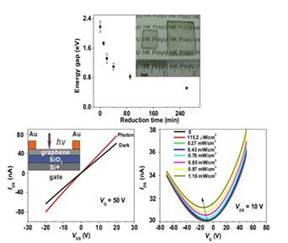
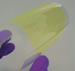
Graphene has shown extraordinary potential in a wide variety of applications including electronics, sensors, actuators, and composites because of its light weight, chemical stability, and unique mechanical and electronic properties. Currently, we are focusing on developing novel methods and strategies to preparation of single- or few- layer graphene or graphene-based composite materials and their applications in electronic and optical devices.
|
| |
| Recent Publications |
| |
Thin Film Field-Effect Phototransistors from Bandgap-Tunable, Solution-Processed, Few-Layer Reduced Graphene Oxide Films
H. Chang, Z. Sun, Q. Yuan, F. Ding, X. Tao, F. Yan, Z. J. Zheng*, Adv. Mater. 2010, 22, 4872. |
|
| |
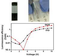
A Transparent, Flexible, Low-Temperature, and Solution-Processible Graphene Composite Electrode
H. Chang, G. Wang, A. Yang, X. Tao, X. Liu, Y. Shen, Z. J. Zheng*, Adv. Funct. Mater. 2010, 20, 2893. |
|
| |
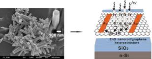
A highly sensitive ultraviolet sensor based on a facile in situ solution-grown ZnO nanorod/graphene heterostructure
H. Chang, Z. Sun, K. Y.-F. Ho, X. Tao, F. Yan, W.-M. Kwok. Z. J. Zheng*, Nanoscale, 2010, 3, 258. |
|
|
|
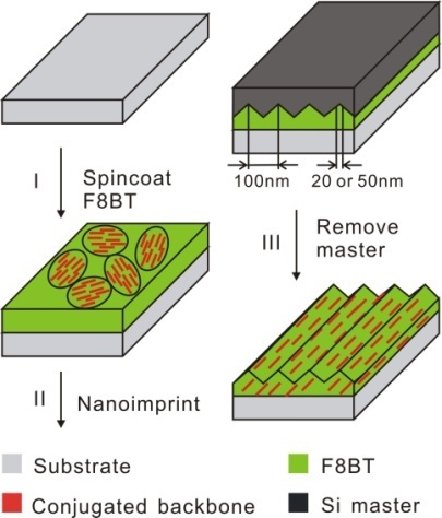
3. Structuring polymer architecture |
Controlling the nanostructures and molecular ordering of polymers are critical in polymer electronic devices. We are interested in developing both chemical and physical approaches to construct the architectures of polymer layers and to control their molecular behaviors. Many of the new structures often lead to new functionality or improvement of devices. A few examples are given below. |
| |
| Recent Publications |
Polymer lateral phase separation:
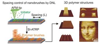
Fabrication of Arbitrary Three-Dimensional Polymer Structures by Rational Control of the Spacing between Nanobrushes
X. Zhou, X. Wang, Y. Shen, Z. Xie, Z. J. Zheng*, Angew. Chem. Int. Ed. 2011, DOI: 10.1002/anie.201102518. |
|
| |
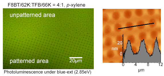
Polymer lateral phase separation:
Surface-Directed Phase Separation of Conjugated Polymer Blends for Efficient Light-Emitting Diodes
K.-H. Yim, Z. Zheng, R. H. Friend, W. T. S. Huck, J.-S. Kim, Adv. Funct. Mater. 2008, 18, 2897. |
|
| |
Polymer multi-layers:
Efficient Conjugated-Polymer Optoelectronic Devices Fabricated by Thin-Film Transfer-Printing Technique
K.-H. Yim, Z. Zheng, Z. Liang, R. H. Friend, W. T. S. Huck, J.-S. Kim, Adv. Funct. Mater. 2008, 18, 1012. |
|
| |
Polymer chain alignment:
Uniaxial Alignment of Liquid-Crystalline Conjugated Polymers by Nanoconfinement
Z. Zheng, K.-H. Yim, M. S. M. Saifullah, J.-S. Kim, R. H. Friend, M. E. Welland, W. T. S. Huck, Nano Lett. 2007, 7, 987. |
|
| |
|
4.
Wearable electronics |
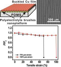
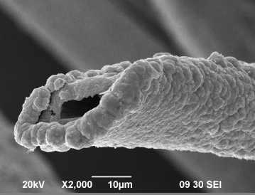
Wearable electronics has received increasing interest in recent years because of its attractive applications in communications, actuations, energy, data management, and biological sensors for medical purposes. The integration and design of wearable electronics into electronic textiles are also recognized as a revolution of the fashion world. We are interested in implementing the state of the art of nanotechnologies and nanomaterials into this new area. One of the projects we are currently exploring is a novel way of making electrical yarns, which are inevitable in all wearable electronics. |
| |
Stretchable conductors with ultra-high tensile strain and stable metallic conductance enabled by pre-strained polyelectrolyte nanoplatforms
X. Wang, H. Hu, Y. Shen, X. Zhou, Z. J. Zheng*, Adv. Mater. 2011, DOI: 10.1002/adma.201101120. |
|
| |
Polyelectrolyte-Bridged Metal/Cotton Hierarchical Structures for Highly Durable Conductive Yarns
X. Liu, H. Chang, Y. Li, W. T. S. Huck, Z. Zheng*, ACS Appl. Mater. Interfaces 2010, 2, 529 . |
|
| |
| |
| |
|