

Issue 2

Vibrant@FENG - Issue 2 (December 2021)
Lab-on-a-chip device for ultrasensitive detection of biomarkers
Professor ZHANG A-ping and Professor TAM Hwa-yaw and their research team in the Department of Electrical Engineering have independently developed three digital ultraviolet exposure/lithography platforms, with which they have developed many advanced optical processing technologies, such as optical 3D µ-printing and precision photoreduction technologies, for the development of photonic devices and sensors with high value-added functions.
 For instance, they developed an optofluidic biochip with high-quality polymer WGM microlaser sensors for ultrasensitive Enzyme-Linked Immunosorbent Assay (ELISA)-based detection of biomarkers. In house optical 3D µ-printing technology was used to fabricate low-threshold WGM microlasers rapidly. The fabricated WGM microlasers were integrated with optical fibres on a microfluidic chip and then modified in situ with biomolecules for biomarker detection. It was demonstrated that such an optofluidic biochip enables on-chip optofluidic ELISA of the disease biomarker vascular endothelial growth factor at an extremely low concentration level of 17.8 fg/mL, which is over 2 orders of magnitude better than the ability of current commercial ELISA kits. The work was published in the journal Lab on a Chip (IF: 6.77) and featured on the Front Cover of the journal.
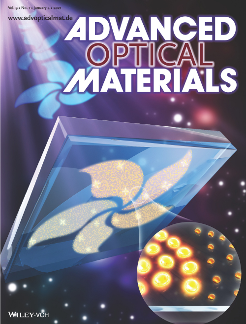 To exploit the extraordinary optical properties of gold nanoparticles (AuNPs), the team developed a method for directly printing micrometer-scale patterns of size-controlled AuNPs. Using in-house digital ultraviolet lithography, a precision photoreduction technology was developed for the light-controlled growth of AuNPs to create micrometer-scale micropatterns on a titanium dioxide photo catalytic layer. The titanium dioxide thin layer not only enables a photo catalytic reduction process for high-precision printing of size-controlled AuNPs in an additive manner, but also introduces a Fano resonance that can sharpen the spectral width of the localised surface plasmon resonance peak and increase its peak-to-valley value. This printing technology can be used to fabricate size-scalable micropatterned plasmonic substrates of size-controlled AuNPs cost-effectively and thus offers new opportunities to develop various types of miniature plasmonic devices ranging from plasmonic biochemical sensors to plasmonically enhanced photothermal and photo-voltaic microdevices. The work was published in the journal Advanced Optical Materials (IF: 9.93) and featured on the Front Cover of the journal.