

Major Theme Stories


Dr Li-Ta HSU
Associate Head and Associate Professor
Limin Endowed Young Scholar in Aerospace Navigation
Department of Aeronautical and Aviation Engineering
PolyU’s Department of Aeronautical and Aviation Engineering (AAE) is in a race against time to diffuse a ticking demographic time bomb that will see the populations of advanced industrialised and urbanised societies age rapidly over the coming two decades, potentially devastating economies.
Its recent ground-breaking advances in the development of Unmanned Autonomous Systems (UAS)—Unmanned Aerial Vehicles (UAV), Autonomous Driving Vehicles, and Unmanned Ground Systems (UGV)—promise to help solve some of the many challenges an ageing society will create, including burgeoning healthcare spending, lower government revenues, and worker shortages. But is the technology progressing fast enough?
“It has to be quick enough, because that's what we need to survive, and that's why our research centre at PolyU exists,” says Dr HSU Li-Ta, Associate Head and Associate Professor, Limin Endowed Young Scholar in Aerospace Navigation. “I’m very optimistic as investment is increasing, which means we can accelerate technology.”
Going grey
Though a global phenomenon, Asia-Pacific is at the forefront of the ageing of urbanised societies. Its population of over 60-year-olds is projected to triple from 2010 to 2050, when one in four people in the region will be aged over 60, according to the United Nations Population Fund. China will reach that milestone much earlier, by 2040, according to the WHO.
The greying of the population will see fewer people enter the workforce, leading to labour shortages and declining government revenues, which will in turn reduce the resources available to fund the higher health care costs associated with an ageing society.
Governments around the world are scrambling to formulate and implement policies intended to future-proof society, with many focusing on the creation of smart cities, which make widespread use of technologically like Artificial Intelligence, robotics, and the Internet of Things to realise the goal of sustainable development.
Up, up, away

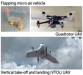
Drawing on the expertise of Professor Chih-yung WEN and Dr LI Boyang, the AAE team has developed various types of UAVs, including flapping micro air vehicles, vertical take-off and landing (VTOL) UAVs, and quadrotor UAVs. The use cases for these autonomous UAVs include search and rescue, parcel delivery, infrastructure inspection and temporal and spatial air quality monitoring.
Recognising these efforts, the Innovation and Technology Commission (ITC) and Electrical and Mechanical Services Department (EMSD) has to date awarded research grants totalling more than HK$8.5 million to AAE to develop in-house UAVs, from design through to testing and production. The team’s successes have also earned AAE notable accolades, such as a Gold Award for Multiple Unmanned Aerial Vehicles (UAVs) Communication Relay Systems by the International Exhibition of Inventions of Geneva in 2017 and a Champion award, Innovation & Search and Rescue Group, at the Taiwan UAV Competition in 2016.
Since 2020, AAE has been working closely with the Environmental Protection Department (EPD) and PolyU’s Research Institute for Sustainable Urban Development (RISUD) to create UAV technologies that will enhance smart city sustainability.
Top gear
As well as exciting advances in the sky, AAE is making headway on the ground too, in the form of Autonomous Driving Vehicles.
For example, Dr HSU and Dr WEN Weisong have been developing a multi-sensor integrated navigation technique for mobile mapping systems that overcomes some of the most pressing challenges in achieving fully automated driving.
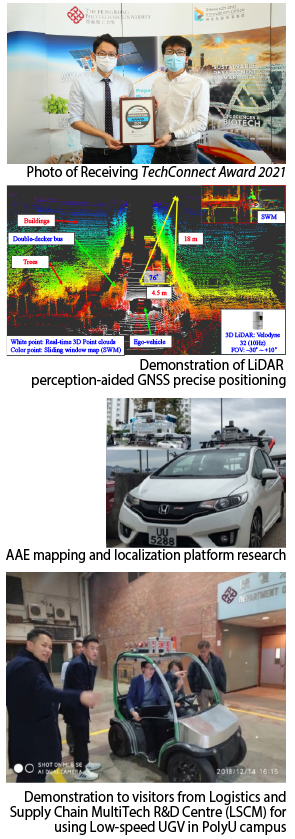
Their award-winning perception-aided sensor fusion algorithm, “3D LiDAR aided GNSS precise positioning for L4 autonomous driving,” is capable of creating a highly accurate map of the complex city landscape and everything in it, otherwise known as a digital twin. The team is in the process of transferring the knowledge to Huawei Technologies.
The technology marries GNSS positioning and LiDAR to overcome a key challenge—obtaining accurate positioning in environments like Hong Kong’s dense urban centre, where signals are diffracted and signal transmission is not direct.
“We tightly connected GNSS technologies with LiDAR technologies to provide an absolute point for all LiDAR so that we can connect all the map together in a big framework, the absolute framework,” says HSU.
Research and developments are being funded by Huawei Technologies, which provided HK$5.5 million, and signed a three-year-long collaborative agreement with AAE. The second phase of the project is underway, scheduled to wrap up in August this year, while a related project, directed by Dr XU Bing, focuses on ensuring the technology is secure against spoofing security attacks, whereby attackers interfere with a positioning signal to present a false location, and is scheduled for completion by November this year.
“To make the research impactful, we need to look at what’s required,” says HSU. “It's about the safety and trustworthiness of the system.
As well as collaborating with Huawei, AAE has teamed up with Beijing-based autonomous driving vehicle company iDriver+ to develop low-speed UGV technology. iDriver+ donated an autonomous driving testing platform to AAE to test and demonstrate the technology.
The combination of AAE’s advances in UAS, industry collaborations and increased funding bode well for the acceleration of technology and the creation of truly smart cities.


Professor Mo YANG
Associate Head (Research) and Professor
Department of Biomedical Engineering
PolyU’s Associate Head of Department of Biomedical Engineering Professor Mo YANG and his research team have harnessed the power of biotechnology and graphene-like nanomaterials to invent new types of nano biosensors that are quicker, cheaper and more sensitive and accurate than anything available today.
“Graphene has super electronic and photoelectronic properties that markedly enhance the performance of biosensing,” says YANG.
The new nano biosensors are applicable to a wide range of scenarios, including the detection of food-borne pathogens, antibiotics, bacterial toxins, and viruses in food and water, and could potentially help improve the health and well-being of populations around the world.
For example, around 2.2 billion people across the world lack access to a supply of clean drinking water, according to UNICEF, with some 1 million people a year dying from preventable water, sanitation and hygiene-related diseases, a high proportion of whom are children, reports water.org. Improved testing through nano biosensors could help identify sources of contamination leading to better health outcomes.
Hard nut to crack
As well as clean water supplies, effective food safety measures are vital to ensure a well-nourished population. An estimated 600 million—about one in 10 people in the world—fall ill after consuming contaminated food annually, and 420,000 die every year from it, “resulting in the loss of 33 million healthy life years”, reports the World Health Organization.
Checking imports of fresh food is time-consuming and risks the degradation of the produce being tested. Not only that, improved accuracy increases the detection rate.
“Governments don’t want to spend several days checking a consignment of fresh fruit, taking samples to the lab and waiting for the results,” YANG says. “So, they need this new kind of rapid biosensor to test food quickly and cheaply on-site.”
New approach
The photoelectrochemical (PEC) biosensing technology YANG has developed relies on light absorption and the interfacial engineering of photoactive materials, which play vital roles in photo-excited electron generation and electron transport, and ultimately boost the performance of PEC biosensing. PEC sensing is highly valued for its simple operation, rapid response, low cost and high accuracy.
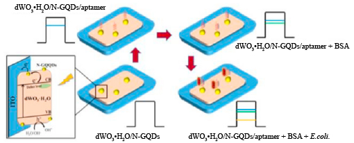
YANG began by developing an ultra-sensitive photoelectrochemical aptamer biosensor for detecting the food-borne pathogen E. coli O157:H7. The sensor is based on nonmetallic plasmonic two-dimensional hydrated defective tungsten oxide nanosheets coupled with nitrogen-doped graphene quantum dots (dWO3•H2O@N-GQDs).
“Graphene was created around 18 years ago, but is only now being put to more widespread innovative uses because of its properties,” says YANG. “We have created a hybrid nano material through pioneering the combined use of nano sheets and graphene quantum dots.”
The limit of detection (LOD) of this PEC aptasensor is 0.05 CFU/mL with a linear detection range from 0.1 to 104 CFU/mL. Moreover, high reproducibility and accuracy were achieved when analyzing milk samples.
The work, which has been published in the renowned Biosensors and Bioelectronics journal, forms a promising foundation for the further development of PEC bioanalysis, and provides valuable data and insights on non-metallic plasmonic materials-based heterojunctions for high-performance PEC biosensing.
Tackling antibiotic resistance
One such avenue of research is detecting the overuse of antibiotics in food.
“Antibiotics are deployed to combat bacteria, but there are too many being used, which can cause the emergence of antibiotic-resistant bacteria. This is a huge issue as antibiotic-resistant bacteria are essentially untreatable,” notes YANG.
Today, antibiotic-resistant bacteria contribute to some 700,000 deaths globally, according to The Lancet, and that figure is forecast to rise rapidly in the near future.
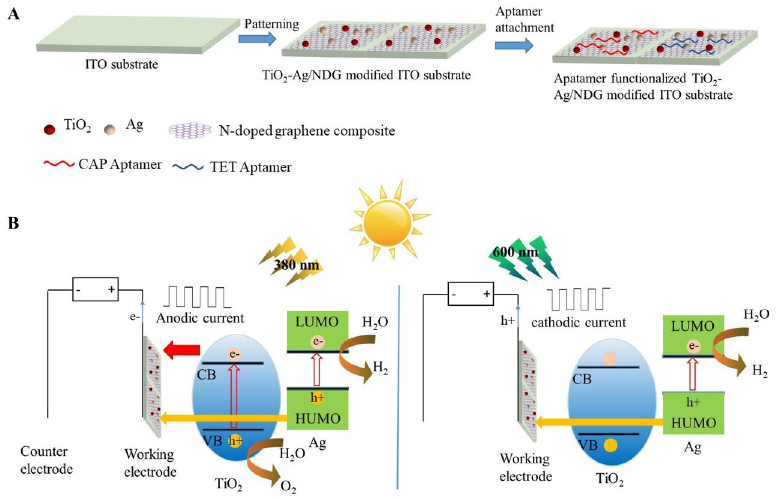
YANG’s team recently developed a wavelength-regulated switchable photoelectrochemical system for the concurrent detection of dual antibiotics.
Its wavelength-dependent PEC sensing strategy is capable of concurrently detecting chloramphenicol (CAP) with a wide linear detection range from 50 pM–10 nM under irradiation of 380nm, and tetracycline (TET) with a linear detection range from 100 pM to 100 nM under irradiation of 600nm, respectively. The limits of detection (LOD) for CAP and TET were 16.7 pM and 30 pM, respectively.
Moreover, the PEC sensor achieved good specificity and outstanding reliability in real-world sample applications.
This wavelength-dependent PEC technique, which has also been published in Biosensors and Bioelectronics, could be conveniently adapted to other food safety biosensing and environmental monitoring applications.
“For example, it would be useful in locations like Hong Kong where high levels of imported seafood are consumed. Exporters in other countries don’t want their fish to die en route, so they have an incentive to overuse antibiotics,” says YANG.
Myriad possibilities
Highly accurate, portable bio sensing solutions can also detect the toxins that bacteria secrete, which is important as treating food with high temperatures kills pathogens, but leaves behind the chemicals they produce.
Monitoring seawater quality is another potential application that could improve aquaculture efficiency as well as better ensure the quality of fish that’s consumed.
“Biosensing could be deployed to monitor the seawater, the live fish, and fish meat when it’s harvested,” YANG says.
From lab to market
While the concept has been proven, more work needs to be done to commercialise it.
“We still need to solve several challenges, such as how to mass produce the technique, before it can be released on the market,” says YANG, noting that the team has already applied for a patent.
YANG and his team’s nano biosensor achievements have won gold medal awards at the World Exhibition of Innovation in 2009 and 2017, and are laying the groundwork for many exciting breakthroughs to come.
Professor ZHANG Aping
Professor
Department of Electrical Engineering
The world is in the grip of a severe shortage of microelectronic and photonic chips, the result of ballooning demand and scant supply caused by supply chain disruption, which is having a knock-on effect on the availability of the myriad products that rely on these essential components, from cars and smartphones to optical communication systems.
But a new digital optical lithography technology, pioneered by Professor ZHANG Aping at the Department of Electrical Engineering (EE), promises to revolutionise photonic chip production by drastically speeding up the R&D and manufacturing processes, in turn reducing costs.
New horizon
For the past 60 years, traditional photolithography has been the workhorse of semiconductor chip production technique. It relies on the use of a photomask, through which ultraviolet light transfers patterns on to the wafer’s photoresist in a process that is costly and time-consuming to deploy. A photomask can cost upwards of US$1 million.
ZHANG developed a digital ultraviolet lithography technology that can rapidly fabricate high-quality low-loss optical waveguides on photonic chips without the need of a photomask.
“The process is akin to replacing the film in a camera with a digital memory stick,” says ZHANG. “Our digital lithography technique employs a high-speed spatial light modulator with millions of micron-size mirrors to replace the photomask for optical exposure processes."
Algorithmic secret sauce
The technology has been a decade in the making, and involved the EE team surmounting several fundamental hurdles.
“Lithography plays a crucial role in advanced manufacturing. All microelectronic chips are manufactured through an exposure process that relies on the use of an expensive photomask, which creates R&D bottlenecks. When new products are designed, they require the creation of a customised photomask, resulting in a long lead time,” says ZHANG. “With digital lithography, which makes use of a virtual mask that relies on algorithms instead of a photomask to create the desired pattern, we don’t need to wait.”
ZHANG has developed specialised algorithms, such as grey-scale dynamic exposure, seamless pattern stitching and optical proximity correction methods, that achieve the ultrafine fabrication of large-scale optical waveguide devices with very low optical propagation loss.
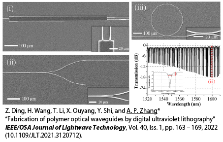
“Our solution needed to be high precision, high accuracy, very high speed and cover a large area,” ZHANG notes. “Therefore, we created a very uniform UV light beam to produce highly precise images, and a system to synchronise many equipment to create images with a huge number of pixels. We’ve achieved optical resolution of 290 nanometer in the fabrication of photonic chip at inch level or larger.”
Each digital micromirror device has about 2 million pixels—for photonics chips, the number of pixels is much larger than 2 million, at the level of billions or even more.
“When creating patterns on chips, the vertical positioning accuracy between the substrate and optical engine needs very high, around 1 micrometer,” says ZHANG. “We use structured light and machine vision to inspect the substrate’s levelness to ensure this level of precision.”
The new lithography technology enables the speedy fabrication of photonic chips by using all-digital processes, including computer-aided chip design, pattern data generation and conversation, and automated light-pattern generation and exposure, and thus is set to fast-track the development of lightwave circuit devices. The use-cases for this technology are widespread. For example, silica-based planar lightwave circuits (PLC) are vital components in devices used in optical fibre communication systems.
Sustainability gains
Photonic chips are not the only application of the cutting-edge digital optical technology advances achieved at PolyU—they are also being used to develop innovative plasmonic devices that reduce the use of precious metals, such as gold and silver.
For instance, ZHANG’s team has developed a revolutionary optical printing technology, named precision photoreduction, that directly prints micropatterns of size-controlled gold nanoparticles (AuNPs) via a digital light controlled nanoparticle-growth method.
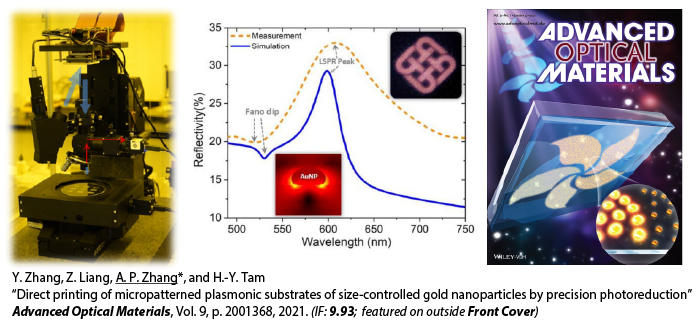
The special additive printing technology reduces the use of expensive gold, which has excellent chemical stability and biocompatibility properties, and thereby opens up a new avenue for the exploration of explore AuNPs-based plasmonic applications.
“Traditional technology uses a deductive process, which etches out the structure. But that creates waste. Our process is the opposite—we expose the area we need, and use particles to grow the pattern,” ZHANG says.
The EE team’s work has been supported for four consecutive years by The Research Grants Council of Hong Kong’s General Research Fund (GRF), and the above mentioned research outcomes has been published on IEEE Journal of Lightwave Technology and Advanced Optical Materials that was highlighted on outside Front Cover.
Though various kinds of digital optical technologies are functioning the modern world, it is the radical new technology that the EE team’s progress makes possible that will most profoundly shape tomorrow’s world.